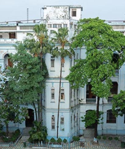
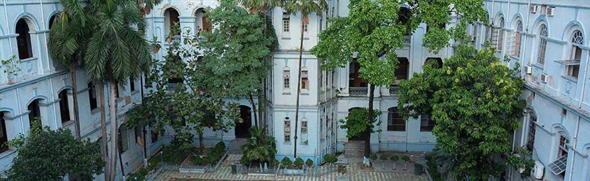
Year of Establishment : December 15, 1984
History of the department : The Department of Electronic Science, University of Calcutta, was established on December 15, 1984. University Grant Commission (UGC) and Department of Electronics (DOE), Govt. of India jointly decided to introduce a 2-year M. Sc. course in Electronic Science with a view to bridge the gap between science and technology in the area of Electronics to develop Human Resources to cater the needs of both Research and Development (R & D) and Industry sectors. It is a DST-FIST and DST-PURSE Sponsored Department. The department has completed its glorious journey of 42 years with its full capacity.
| Name | Designation | Area of specialisation | Email/Phone number |
|---|---|---|---|
| Anupam Karmakar [Profile] |
Professor | Semiconductor Nano-Science & Nano-Technology, Sensors, Microwave Systems, Circuits & Decices |
akelc@caluniv.ac.in anupamkarmakar@yahoo.co.in akarmakar.cu@gmail.com 033-23603722 Ext. 37 |
| Abhijit Mallik [Profile] |
Professor | Nano-scale CMOS (Classical & Novel), MOS Insulator | abhijit_mallik1965@yahoo.co.in 033-23603722 Extn. 20 |
| Sanatan Chattopadhyay [Profile] |
Professor & Head | Strained-Si and Nano-scale CMOS Devices, High-k Gate Insulator, Nano-science and Nano-technology, Sensors, Communications |
scelc@caluniv.ac.in c_sanatan@yahoo.com 033-23603722 Extn. 25 |
| Jayee Sinha [Profile] |
Assistant Professor | Condensed Matter Physics and material Science | jayee.bhatt@gmail.com jselc@caluniv.ac.in 033-23603722 Extn. 31 |
The Department of Electronic Science offers two academic programs :
| Programme | Level of study | Eligibility | Intake capacity |
|---|---|---|---|
| B.Tech. | Under Graduate | Higher Secondary (10+2) with 60% marks in PCM, and qualifying WBJEE | 30 |
| M.Sc. | Post Graduate | B.Sc. (Hons.) in Electronics/ Physics | 30 |
| Ph.D. | Research | M.Sc. / 4-year B.Sc. with NET or M.Tech. / B. Tech. with GATE |
As per norms |
| Name | Research topic | Name of the supervisor | Date of registration |
|---|---|---|---|
| Akant Sagar Sharma | Studies on III-V Nitride and Bismide semiconductor nano-structure | Prof. Sunanda Dhar | 27/10/2014 |
| Abhijit Banerjee | Some studies on the electrical characteristics of planar Schottky barrier diode | Prof. P.Chattopadhyay | 30/12/2012 |
| Anindita Das | High-K dielectrics | Dr. Sanatan Chattopadhyay | |
| Anirban Roychowdhury | Prof. Somnath Sarkar Dr. Dharmadas Kumbhakar |
02/03/2015 | |
| Anup Karak | Prof. Somnath Sarkar | 10/03/2014 | |
| Arunansu Sadhu | Prof. Somnath Sarkar | 10/03/2014 | |
| Aswini Kumar Mallick | Prof. Somnath Sarkar | 18/05/2012 | |
| Avishek Das | Zinc oxide nano-structures and their photo-diodic applications | Dr. Sanatan Chattopadhyay | |
| Basudev Nag Chowdhury | Ballistic transport in NW-MOSFETs | Dr. Sanatan Chattopadhyay | 04/03/2014 |
| Bazlul Karim | Study of optoelectronic properties of some II-VI thin film semiconductors deposited by chemical bath deposition technique | Prof. P.Chattopadhyay | 18/11/2015 |
| Chirantan Das | Food safety and quality assessment: sensor studies of bio-consumables | Dr. Sanatan Chattopadhyay Dr. Anupam Karmakar |
12/08/2014* |
| Debarup Roy | Prof. Somnath Sarkar Dr. Anupam Karmakar |
04/04/2016* | |
| Debuprasad Haldar | Some studies on the electrical characteristics of semiconductor heterojunction diode | Prof. P.Chattopadhyay | 16/12/2013 |
| Dip Prakash Samajdar | Investigation of the properties of group III-V Bismide semiconductors | Prof. Sunanda Dhar | 10/03/2014 |
| Emona Datta | Prof. Abhijit Mallik | 04/04/2016* | |
| Ivy Dutta | Prof. Somnath Sarkar Dr. Dharmadas Kumbhakar |
02/03/2015 | |
| Jenifar Sultana | Copper oxide thin film based solar cell | Dr. Sanatan Chattopadhyay | 04/04/2016* |
| Jhuma Pal | Some studies on the electrical characteristics of meta-semiconductor field effect transistors | Prof. P.Chattopadhyay | 03/06/2013 |
| Mainak Palit | Nano-electronic device: fabrication and characterization | Dr. Sanatan Chattopadhyay Dr. Amlan Chakrabarti | |
| Mithun Kumar Bhowal | Bi containing III-V bulk layers and low-dimensional structures | Prof. Sunanda Dhar | 14/12/2015 |
| Prosenjit Roychowdhury | Prof. Somnath Sarkar Dr. Sankar Gangopadhyay |
25/06/2013 | |
| Rajib Saha | Nano-structure based memory devices | Dr. Anupam Karmakar Dr. Sanatan Chattopadhyay |
04/04/2016* |
| Rathin Basak | Analytical modeling of tunnel currents in advanced MOS devices | Prof. Abhijit Mallik | 12/07/2012 |
| Sayantan Bakshi | Prof. Sunanda Dhar Dr. Sanatan Chattopadhyay |
04/04/2016* | |
| Shilpi Guin | Device design and performance analysis of novel CMOS devices | Prof. Abhijit Mallik | 12/07/2012 |
| Sk. Masum Nawaj | Random variability study in advanced CMOS devices | Prof. Abhijit Mallik | 02/03/2015 |
| Somdutta Paul | Metal oxide nano-structures: Growth and characterization | Dr. Sanatan Chattopadhyay | 04/03/2014 |
| Subhadip Chakraborty | Bioelectronics: Analytical modeling and bioelectrical studies | Dr. Anupam Karmakar Dr. Sanatan Chattopadhyay |
12/08/2014* |
| Subhasis Das | Optical and electrical characterization of binary and ternary III-V Bismide bulk layer and quantum structure | Prof. Sunanda Dhar | 27/10/2014 |
| Subhrajit Sikdar | Optical photo sensor modeling | Dr. Sanatan Chattopadhyay Dr. Anupam Karmakar |
04/04/2016* |
| Sulagna Chatterjee | Nano-scale strain engineering | Dr. Sanatan Chattopadhyay | |
| Sutanu Dutta | Some studies on electrical and optical properties of metal-semiconductor field effect transistor | Prof. P.Chattopadhyay | 06/09/2013 |
| Swarnali Guha Roy | Some studies on the properties of thin film polycrystalline metal sulfides prepared by chemical methods | Prof. P.Chattopadhyay | 26/06/2013 |
| Utsa Das | Prof. Sunanda Dhar | 04/04/2016* | |
| * Indicates date of enrollment | |||
| Project title | Funding agency | Principal investigator | Duration | Budget |
|---|---|---|---|---|
| Systems Biology and Bio-medical Engineering: Development of Digital Micro-Fluidics Chip | World Bank | Dr. S. Chattopadhyay | 3 years | 1 Crore |
| Design and Development of Crystal Growth System for Preparation of High Pure Gallium Nitride for Light Emitting Diode (LED) and Other Related Optoelectronic Applications | DST, Govt. of India |
Prof. Sunanda Dhar | 3 years | 72.69 Lac |
| Devices Design and Optimization of Complementary Tunnel FETs for Low Power Applications and Their Variability Study | DST, Govt. of India |
Prof. A. Mallik | 3 years | 40.59 Lac |
| Title of the programme | Principal collaborator of The department | Name and address of the collaborating institution | Principal collaborator of the collaborating institution | Duration of the programme |
|---|---|---|---|---|
| DST project “Design and development of crystal growth system for preparation of high pure gallium nitride for light emitting diode (LED) and other related optoelectronic applications” | Prof. Sunanda Dhar | Centre for Materials for Electronic Technology (C-MET), Cherlapally, Hyderabad | Dr. V. N. Mani, Scientist-E | 3 years |
| Electrical Characterization Facility | Purpose |
|---|---|
| Keithley Pico-Ammeters (4) (SMU) | Current Measurement System |
| 4200 SCS Parameter Analyzer | Electrical Measurement |
| Liquid Nitrogen Electrical Probe Station | Wafer Level Probing |
| Keysight LCR | Capacitance Measurement |
| Boonton 7200 Capacitance Meter | Capacitance Measurement |
| TEGAM LCR Meter | Capacitance Measurement |
| Impedance Analyzer | Electrical Measurements |
| Cyclic Voltameter | Electrical Measurements |
| Solar Simulator | Solar Cell Measurements |
| Monochromator | Optical Characterizations |
| Photoluminescence (PL) Systems | Optical Characterizations |
| Optical Bench | Optical Characterizations |
| DPSS Laser 50 mW | Optical Characterizations |
| DPSS Laser 100 mW | Optical Characterizations |
| Displex Closed Cycle Helium Cryogenic System | Produces 10 k temperatures |
| Contact Measurement Setup | Digital Microfluidics |
| Fabrication Facility | Purpose |
|---|---|
| Chemical Bench | Chemical Processing |
| Fume Hood | For Safe Processing |
| Millipore Deionized Water Systems (2) | Wafer Cleaning |
| Growth Furnaces (2) | Thin Film Growth |
| Annealing Furnaces (2) | Thermal Annealing |
| Vacuum Coating Units (3) | Film Growth/Metal Contact |
| High Vacuum Evaporators | Film Growth for Device |
| Dual Gun Sputtering System | Film Growth |
| Rapid Thermal Annealing System | Sample Annealing |
| Indigenously developed Lithography System | Device Fabrication |
| CBD Growth System | Nanostructures Growth |
| Spin Coater | Film Growth |
| High Power Microscopes | Inspection |
VLSI Design Centre (RUSA 2.0)
Campus : Rashbehari Siksha Prangan (Rajabazar Science College Campus)
Address for communication : Department of Electronic Science, Meghnad Saha Bhavan, 92, A.P.C Road, Kolkata-700 009